High-performance, highly integrated A+C dual-port fast charging chip HUSB365 for miniaturized multi-port PD3.1 fast charging source design
2 7, 2023
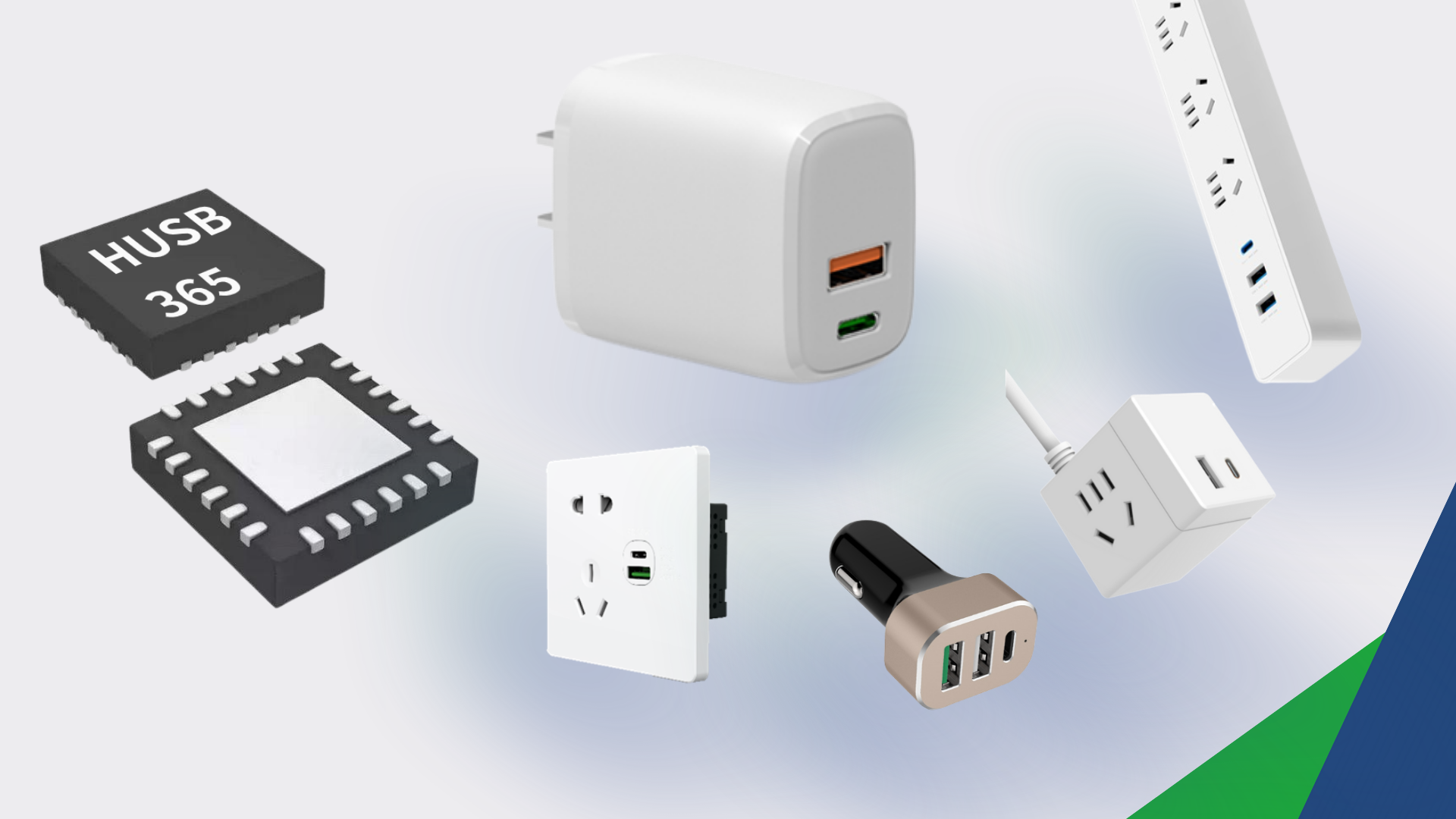
With its advantage of supporting users to charge multiple electronic devices at the same time, multi-port fast charging has become the newest addition to the fast charging source market. In response to this trend, Hynetek has launched HUSB365, a dual-port A+C fast charging chip.
HUSB365 is a high-performance, highly integrated USB Type-C and USB Type-A dual-port controller, which supports fast charging when either A-port C port is working alone; the voltage returns to 5V when A-port C port is working at the same time. HUSB365 is suitable for 15W~65W multi-port 1A1C, 2A2C, 1A2C, 2A1C and other fast Charging source design, such as power adapter, car charger, etc. HUSB365 integrates Chip-Link technology to enable chip communication through a single PIN (FC-PIN) for more applications, such as dual USB Type-C or dual USB Type-A applications.
The HUSB365 integrats PD3.1 controller which supporting 5 FPDOs and 2 APDOs. The 5 FPDOs support programmable current and 2 APDOs support programmable voltage and current for different applications. All of PDOs are fully compliant with PD3.1 Rev.1.3 spec. Besides, the HUSB365 also supports BC1.2 DCP, Apple 2.4A, QC2.0/3.0/QC3+, AFC, FCP and SCP, PE1.1+ protocols. The HUSB365 integrates all of required protections such as Over Voltage Protection (OVP), Under Voltage Protection (UVP), Under Voltage Lock Out (UVLO), Over Current Protection (OCP), Fast Over Current Protection (FOCP), CC or DPDM Over Voltage Protection (Port OVP) and Thermal Shut Down (TSD). It is available in 4 mm x 4 mm, QFN-24L package.
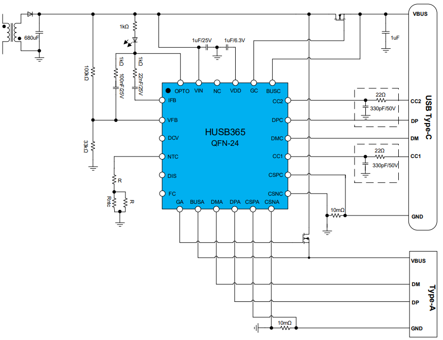
Figure 2. Typical Application Circuit for ACDC
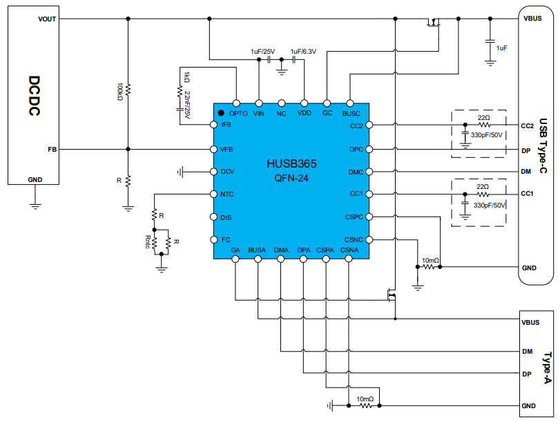
Figure 3. Typical Application Circuit for DCDC
FEATURES
USB Type-C 2.1 and USB PD3.1 Compliant
Support 5V, 9V, 12V, 15V and 20V five FPDOs
Support 2 Programmable APDOs available
Support BC1.2 DCP and HVDCP protocols
BC 1.2 DCP Mode – Apple 5V 2.4A Mode
QC2.0/3.0/QC3.0+ Class A or Class B
Samsung AFC – FCP and LVSCP/HVSCP
PE 1.1+
Support USB Type-A and Type-C DualPort Working Mode
Support Chip-Link
Support as low as 10mA Lightload threshold
External N-MOSFET Supported
Support Constant Voltage Loop(CV) and Constant Current Loop(CC) Operation
Support Line Loss Compensation
Integrated VIN and VBUS Fast Discharge
Integrated OVP, UVP, UVLO, OCP, FOCP, CC/DPDM OVP, TSD and NTC Protections
Support Online Upgrade
QFN-24L (4mm x 4mm) Package
±4kV HBM ESD Rating for USB IO Pins
HUSB365-based 1A1C fast charging source design

The HUSB365-based 1A1C fast charging source design realizes the need for a single chip to control dual-port fast charging, which can greatly reduce BOM costs. In addition, HUSB365 can judge the threshold at low light load, which can perfectly solve the problem of filling up small current devices; HUSB365 can also automatically identify whether the cable or the device, which can enhance the fast charging experience.
HUSB365-based 2A2C fast charging source design
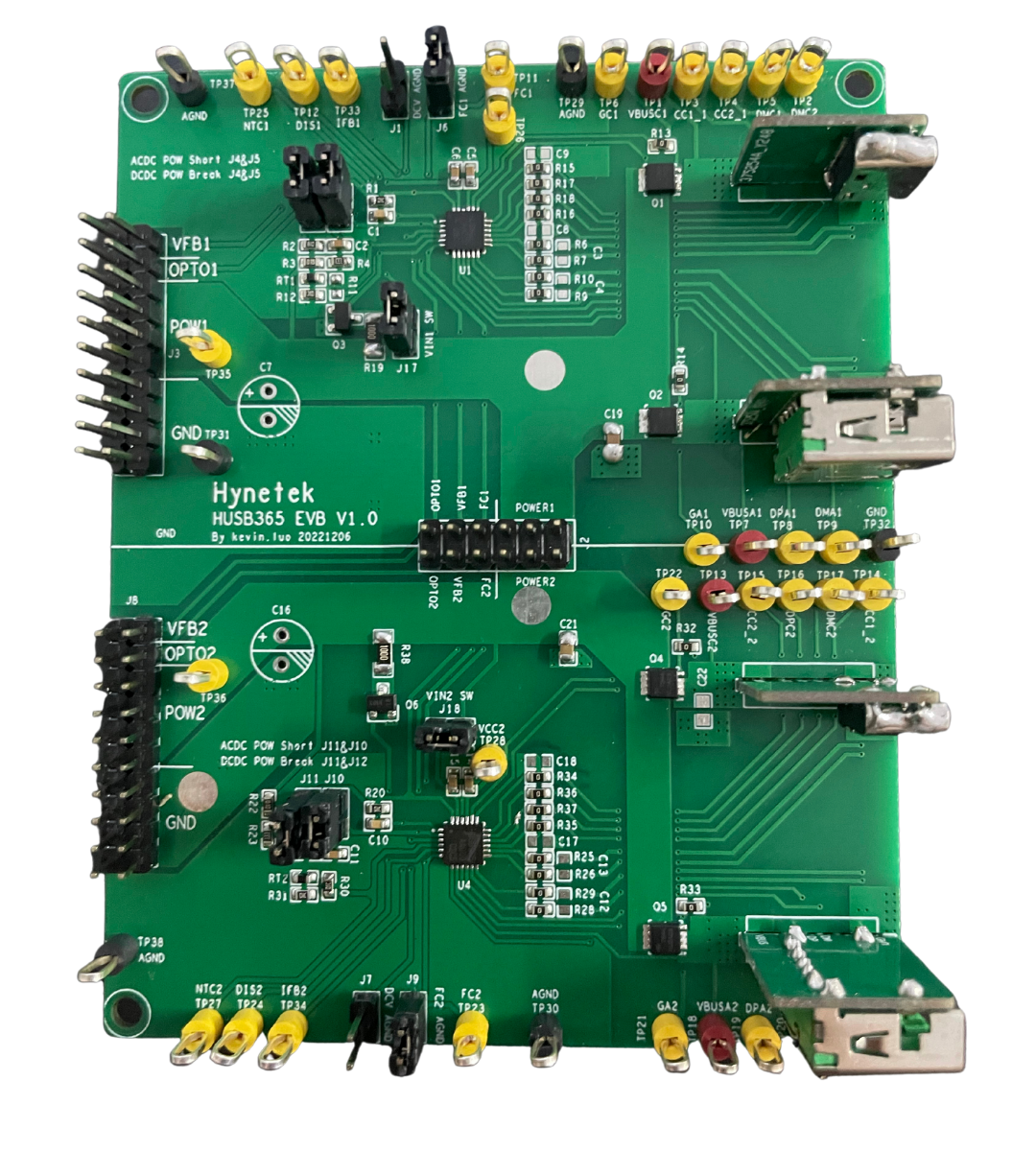
Currently, the multi-port fast charging sources on the market are mainly designed according to three architectures: fully shared architecture, fully independent architecture, and semi-independent architecture. HUSB365 supports 1A1C or 2A2C and more A+C ports with fully shared architecture, and supports 15W~65W fast charging when each port is working separately and 5V charging when working simultaneously. With HUSB365, you can also flexibly implement 1A2C, 2A1C and more fast charging designs, welcome to contact us for more information.


