New Solution for Computing Power Supply Challenges
11 10, 2025
At the recent OCP Global Summit, NVIDIA officially released a white paper outlining the next phase of development for AI factory power infrastructure. This new architecture innovatively shifts from traditional 415 VAC or 480 VAC alternating current to an end-to-end 800 VDC direct current bus. By eliminating redundant AC-to-DC conversion stages, it delivers high-voltage direct current directly to compute nodes. This approach not only significantly reduces transmission losses but also saves up to 26% in space compared to traditional multi-stage conversion solutions. Within the hierarchical power architecture of data centers, the 48 V power supply architecture emerges as a key enabler for enhancing system efficiency due to its ability to substantially lower transmission losses.
In 48 V power supply architectures, traditional mainstream solutions employ a two-stage conversion topology: first, an intermediate bus converter (IBC) steps down the 48 V to a 12 V intermediate bus voltage; then, a point-of-load (PoL) converter converts the 12 V to the ultra-low voltages ranging from 0.8 V to 1.8 V required by chip cores such as MCUs, FPGAs, or ASICs. Although individual conversion stages may achieve 96% efficiency, cumulative losses reduce the overall efficiency of two-stage systems to approximately 87%. Furthermore, this architecture requires two separate power conversion modules and corresponding magnetic components, increasing the solution's overall volume and material costs. The longer power path also introduces greater parasitic impedance, impacting dynamic response speed.

Figure 1: Traditional mainstream two-stage power supply solution
In contrast, the single-stage direct conversion architecture directly converts the 48 V input voltage to the target low voltage in a single step. By eliminating intermediate conversion stages, this approach typically achieves overall efficiencies exceeding 90%. Physically, the single-stage conversion saves PCB area and copper foil usage originally allocated for intermediate bus circuits, significantly boosting power density. Its shorter power path also helps reduce loop inductance, thereby optimizing load transient response performance.

Figure 2: Single-stage conversion solution from 48 V to 1 V using the HP1800
Recently, Hynetek introduced the HP1800 PWM phase-doubling controller. This chip expands a single tri-state input PWM signal into four complementary PWM outputs with 180° phase-shifted interleaving. Designed specifically for high-density, high-efficiency DC-DC power supplies, it enables direct expansion from the second-stage multi-phase controller in traditional mainstream two-stage solutions to control a single-stage half-bridge current-doubling rectifier converter with 48 V input. This eliminates the need for additional PWM control signals, significantly reducing the design complexity and cost associated with migrating from two-stage to single-stage topologies. The solution is widely applicable in scenarios such as single-stage Power-of-the-Line (PoL) supplies and isolated/non-isolated DC-DC brick module power supplies.

Figure 3: HP1800 DFN-8L Package and Pinout Diagram
HP1800 Chip Features
Up to 7 V Supply Voltage
Configurable Phase Multiplier as Doubler from A Single PWM Input
Capable of Generating High Output Switching Frequency from 200 kHz to 2000 kHz
Tri-State PWM Input for Power Stage Shutdown
Small Size: DFN2x2-8L Package
Operating Ambient Temperature Range of -40°C to 125°C

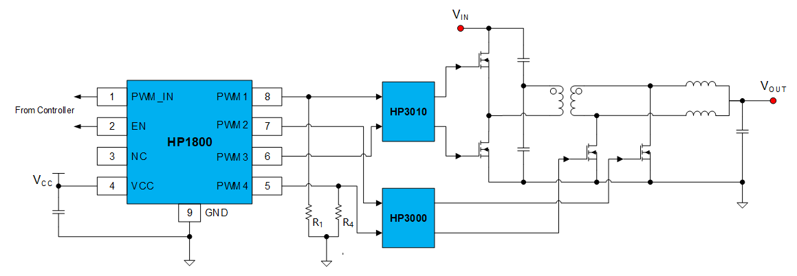
Figure 4: Typical Application Block Diagram of HP1800: Single-Stage 48 V to 1.0 V Half-Bridge Current-Doubling Rectifier Converter

Figure 5: HP1800 Demo Board
Feature Highlight 1: PWM Phase-Doubling Output
The HP1800 expands a single tri-state PWM input signal into four complementary PWM output signals with 180° phase shift, greatly simplifying the design of main power topologies requiring multiple complementary PWM drivers while reducing demands on the main controller's PWM output channels. Additionally, the pull-down resistors for PWM1 and PWM4 enable initialization settings for the dead zones of PWM1/2 and PWM3/4 respectively, allowing flexible adjustment based on actual system requirements.

Figure 6: Timing Diagram for HP1800 PWM_IN Input and PWM1-4 Outputs
Feature Highlight 2: Comprehensive Anti-Disturbance Mechanism
Since the four complementary PWM output signals are controlled by a single PWM input signal, any disturbance or abnormal timing on the PWM input signal may pose a significant threat to the stability of the output signals. In severe cases, this could cause complementary signals to bypass, potentially damaging power devices. The HP1800 optimizes the timing control for PWM input signals entering or exiting the third state and for output complementary signals to effectively handle potential abnormal operating conditions, enabling robust response to sudden external disturbances.

Figure 7: (Left) PWM_IN transitions from the third state to low level and begins output after completing one full PWM pulse; (Right) PWM_IN transitions from the third state to high level and begins output after completing one full PWM pulse.

Figure 8: PWM_IN introduces interference pulses with amplitudes exceeding the signal high/low thresholds.
The figure below shows a typical application circuit for the HP1800 driving a multiphase interleaved half-bridge current-doubling converter. This converter reduces a typical 48 V input voltage to 1.0 V through a single-stage power conversion, significantly improving power conversion efficiency compared to two-stage conversion schemes. The PWM_IN and EN signals are controlled by an external traditional multiphase controller. The PWM1 to PWM4 outputs simultaneously drive the half-bridge driver HP3010 (120 V/3 A, DFN2x2-8L) and the dual-channel low-side driver HP3000 (30 V/5 A, DFN2x2-8L). The initial dead time between complementary signal pairs (PWM1/PWM2 and PWM3/PWM4) can be independently configured via resistors R1 at the PWM1 terminal and R4 at the PWM4 terminal.

Figure 9: Circuit Block Diagram of a Multiphase Interleaved Half-Bridge Current-Doubling Rectifier Converter
After adopting the HP1800, the overall power architecture can be easily transformed from a two-stage to a single-stage design. It achieves direct 48V bus power supply in a single stage using only the multi-phase controller from the original second-stage circuit. The HP1800 offers a new solution for computing power supplies—featuring a simple design and exceptional cost-effectiveness! Engineers are welcome to call for inquiries.


